Nikon NWL-641 IC Inspection Wafer Loader
Nikon Updated: 2007-06-19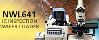
Macro, micro and a whole new level of inspection efficiency.
In addition to micro inspections, Nikon's new M-type automatic wafer loaders feature sophisticated tilt, rotation and flutter modes for enhanced macro inspections. By eliminating operator handling, all NWL-series wafer loaders increase throughput and reduce contamination. The sophisticated vacuum-type mechanical transfer system efficiently copes with distorted wafer carriers.
Simple, Speedy Wafer Exchange
Operation is a breeze, thanks to the logical arrangement of keys on the control panel. The NWL-641 series can memorize up to 10 combinations of wafer channels to be inspected. The orientation flat detector allows the wafer direction to be set in four directions (0°, 90°, 180°, 270°) individually during wafer loading onto the microscope or during wafer unloading. Wafer exchange takes a short two seconds.
360° Rotation Vacuum Wafer Chuck
The vacuum wafer chuck on the stage draws and holds a wafer transferred by the loader, and if necessary, the wafer can be rotated 360° by using the syringe rotation knob, allowing the loaders to meet the varying needs of microscopic inspection.
Enhanced Macro Observations with Fluttering Mode
The NWL-641 has an option that incorporates sophisticated macro observation movements, including Nikon’s original fluttering mode, tilt macro rotation, and fluttering + tilt macro rotation.
Irregular-Shaped Wafer Cassette Capability
The loader in the NWL-641 series uses transmission-type laser wafer sensors. These sensors check the presence of wafers in the cassette, wafer tilt, as well as wafer deformation, to determine automatically the ideal position in which to take the wafers in and out, thus ensuring secure transfer.
Anti-Contamination Design
To significantly curtail dust generation from the equipment and the attachment of particles to wafers, Nikon adopted a special design, whereby the motor unit in the macro mechanism is located as far apart as possible from the wafer under inspection.
There are no manuals currently available for this model.
Related Manuals
Nikon NWL-860 IC Inspection Wafer Loader
Nikon MM400/800 Industrial Measuring Microscopes
Nikon Eclipse C1si Confocal Microscope System
Nikon Eclipse L200 Series IC Inspection Microscopes
Nikon Eclipse L300 Series FPD/LSI Inspection Microscopes
Nikon Eclipse C1 Plus Confocal Microscope System
Nikon Eclipse LV150 Series Industrial Microscopes
Nikon LiveScan SFC Swept Field Confocal Microscope
Nikon SMZ1500 Zoom Stereomicroscope
Nikon Epiphot 200 Inverted Metallograph Microscopes
Nikon SMZ1000 Zoom Stereomicroscope
Nikon Epiphot 300 Inverted Metallograph Microscopes